Precision Thin Film Deposition Materials
AEM Deposition delivers ultra-high purity sputtering targets, evaporation materials, substrates, and crystal products for advanced thin film applications in optics, semiconductors, solar, and research.
This page is not the official website. Generated by AI, does not constitute any advice. If needed, please click here to visit the corresponding official website.
AEM Deposition delivers ultra-high purity sputtering targets, evaporation materials, substrates, and crystal products for advanced thin film applications in optics, semiconductors, solar, and research.
AEM Deposition is a leading provider of high-purity materials for thin film deposition technologies. With a focus on innovation and quality, we serve industries ranging from semiconductor manufacturing and solar energy to optical coatings and advanced research laboratories.
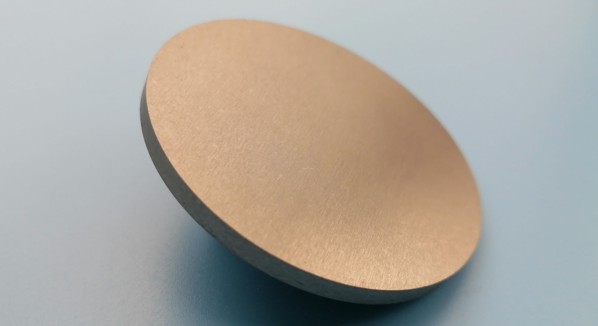
Our product portfolio includes sputtering targets, evaporation materials, crucibles, thin film substrates, and specialty crystals engineered to meet the most demanding performance standards.
Max Purity Level
Global Markets
Industry Experience
Products Available
Comprehensive selection of high-purity materials for physical vapor deposition (PVD), chemical vapor deposition (CVD), and molecular beam epitaxy (MBE) processes.
Purity: 99.999%
Size: 2" diameter x 0.25" thickness
Price: $60/pc
Purity: 99.95%
Size: 2" diameter x 0.25" thickness
Price: $70/pc
Purity: 99.999%
Size: 2" diameter x 0.25" thickness
Price: $60/pc
Purity: 99.999%
Size: 2" diameter x 0.25" thickness
Price: $60/pc
Type: Semiconductor
Diameter: 2", Orientation: (100)
High resistivity GaAs wafers for epitaxial growth
Material: Pure Tungsten
Grade: W1, High Density
Ideal for electron beam evaporation systems
Purity: 99.999%
Form: 3mm diameter x 2mm height
Used in ITO and compound semiconductor deposition
Material: YSZ
Size: 20mm x 10mm (OD x H)
High temperature resistance up to 2200°C
Type: Nonlinear Optical
Orientation: Z-cut, Size: 10x10x0.5mm
For modulators, frequency doublers, and sensors
Purity: 99.95%
Size: 3" diameter x 0.125" thickness
Used in solar cell and semiconductor applications
Purity: 99.999%
Form: 3mm cubes
For IR coating and semiconductor doping
Composition: In2O3:SnO2 (90:10)
Purity: 99.99%, Size: 2" diameter
Transparent conductive oxide for displays and solar cells
Our materials enable innovation across critical technology sectors.
Anti-reflective coatings, mirrors, filters, and optical components requiring high-purity deposition materials with precise stoichiometry and low defect density.
Materials for photovoltaic cells including CIGS, perovskite, and thin-film silicon solar technologies, with high deposition efficiency and uniformity.
Interconnects, barriers, and seed layers for semiconductor devices using high-purity copper, tantalum, titanium, and other advanced materials.
Ultra-high vacuum compatible materials with extremely low outgassing rates for synchrotron beamline components and scientific instrumentation.
Wear-resistant and aesthetically pleasing coatings for tools, automotive parts, and consumer products using nitrides, carbides, and diamond-like carbon.
Custom materials and small-batch production for academic and industrial R&D in nanotechnology, quantum materials, and next-generation devices.
Materials with purity levels up to 99.999% (5N) and strict impurity control for critical applications.
Tight dimensional tolerances and surface finishes optimized for consistent deposition performance.
One of the broadest selections of deposition materials covering metals, alloys, oxides, and specialty compounds.
Dedicated technical support and logistics network serving customers in research institutions and manufacturing facilities worldwide.
We offer sputtering targets with purity levels ranging from 99.9% (3N) to 99.999% (5N), depending on the material. High-purity materials are available for semiconductor and research applications.
Yes, we specialize in custom fabrication and can produce materials in various sizes, shapes, and configurations to meet your specific equipment requirements.
Standard products typically ship within 1-2 weeks. Custom orders may require 3-6 weeks depending on complexity. We provide exact lead times upon inquiry.
Yes, we provide target bonding services for planar and rotary targets using indium or other suitable solders to ensure optimal thermal and electrical contact.
Our materials are packaged in cleanroom conditions using anti-static, vacuum-sealed containers with desiccants to prevent contamination and oxidation during shipping.
Contact us for product inquiries, technical support, or custom material requests.
Notice for Buyers: If you are a buyer, the above information is generated by AI collection and does not constitute any advice. If necessary, please visit the corresponding official website.
For Domain Owners: If you are the domain owner and do not want to be included by fobcompany.info, please contact support@fobcompany.info via your corporate email to cancel. We will cancel your inclusion within 3 business days.
如果您是域名所有者 不想被fobcompany.info收录 请用企业邮箱联系support@fobcompany.info 取消收录 我们将在3个工作日取消您的收录
Service Request: If you are other domain and want to be included, please contact support@fobcompany.info
如果您是其他域名合作 也请联系support@fobcompany.info